PIN- Diodes
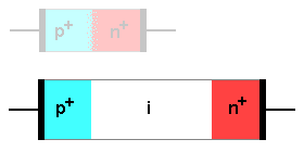
| normal semiconductor positive-negative diode: |


|
| a semiconductor positive-intrinsic-negative (PIN) diode: | |
| p- region (high-doped) i-region n-region |
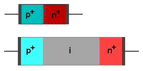
Figure 1: Structure of a pin-diode
The pin diode consists of two narrow but highly doped, semiconductor regions separated by a thicker, lightly-doped material called the intrinsic region. As suggested in the name, pin, one of the heavily doped regions is p-type material and the other is n-type. The same semiconductor material, usually silicon, is used for all three areas. Silicon is used most often for its power-handling capability and because it provides a highly resistive intrinsic (i) region. The pin diode acts as an ordinary diode at frequencies up to about 100 megahertz but above this frequency the operational characteristics change.
The large intrinsic region increases the transit time of electrons crossing the region. Above 100 megahertz, electrons begin to accumulate in the intrinsic region. The carrier storage in the intrinsic region causes the diode to stop acting as a rectifier and begin acting as a variable resistance.
When the bias on a pin diode is varied, the microwave resistance changes from a typical value of 6 kiloohms under negative bias to about 5 ohms when the bias is positive. Thus when the diode is mounted across a transmission line or waveguide, the loading effect is insignificant while the diode is reverse biased, and the diode presents no interference to power flow. When the diode is forward biased, the resistance drops to approximately 5 ohms and most power is reflected. In other words, the diode acts as a switch when mounted in parallel with a transmission line or waveguide. Several diodes in parallel can switch power in excess of 150 kilowatts peak. The upper power limit is determined by the ability of the diode to dissipate power. The upper frequency limit is determined by the shunt capacitance of the pn junction. Pin diodes with upper limit frequencies in excess of 30 gigahertz are available.
