Analogue-to-Digital Converter
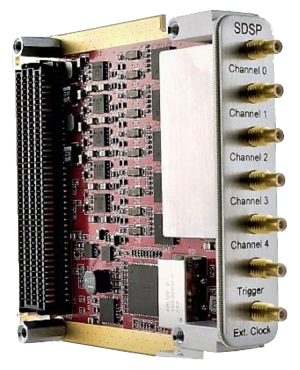
Figure 1: Example of an FMC module with 5 ADC channels each running at up to 500 MS/s with a dynamic range of 16 bits.
(Courtesy of Sundance DSP Inc., www.sundancedsp.com)

Figure 1: Example of an FMC
module with 5 ADC channels each running at up to 500 MS/s with a dynamic range of 16 bits.
(Courtesy of Sundance DSP Inc.,
www.sundancedsp.com)
Analogue-to-Digital Converter
Analogue-to-Digital Converter don't operate continuously but sample the analog signal at diskrete intervals Ts= 1/ fs and convert the sampled signal to digital form.
Converter (ADC)
Converter (ADC)
Approximation

Converter (ADC)
Nyquist-Shannon Sampling Theorem
When sampling a signal at discrete intervals the sampling frequency fmax must be greater than twice the highest frequency fmax of the input signal in order to be able to reconstruct the original perfectly from the sampled version.
The minimum sampling frequency fs that allows reconstruction of the origin signal is known as the Nyquist frequency. Sampling at less than the Nyquist frequency causes aliasing.
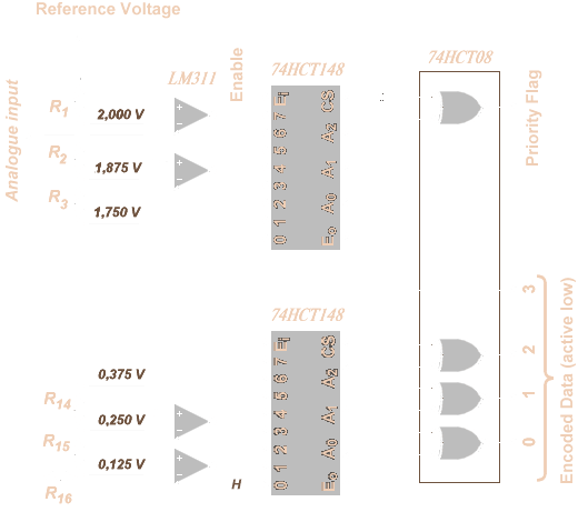
Figure 2: Diagram of a 4-bit flash ADC with 15 comparators
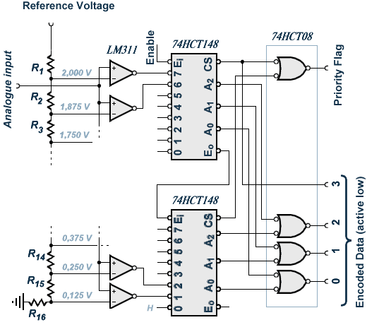
Figure 2: Diagram of a 4-bit flash ADC with 15 comparators

Figure 2: Diagram of a 4-bit flash ADC with 15 comparators
Flash ADC
Flash converters are so-called because they are the fastest type of ADC. Flash ADCs contain a chain of parallel comparators. They can be obtained with a limited precision only, are expensive and consume a considerable amount of pover. The output of the comparators is converted to binary form by combinational logic (a priority encoder).
Flash ADCs perform 2n-1 single-bit conversion in parallel. For the integrated ADC e.G. Maxim MAX104 with 8 Bit encoded data you need 255 comparators and it costs about 900 €. It has got a conversion time of 1 Nanosecond (1 Gsps).
Half-flash ADC
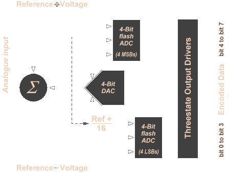
Figure 3: Principle of an 8-bit half-flash ADC
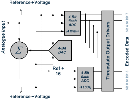
Figure 3: Principle of an 8-bit half-flash ADC

Figure 3: Principle of an 8-bit half-flash ADC
By performing the conversion in two steps it is possible to reduce the complexity of flash converters, at the expense of some loss of speed. This half-flash converter uses 30 comparators to achieve an 8-bit precision, compared with 25530 comparators for a full 8-Bit flash ADC.
Tracking ADC
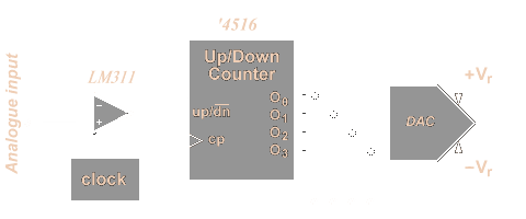
Figure 4: Principle of an 4-bit tracking ADC
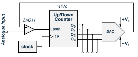
Figure 4: Principle of an 4-bit tracking ADC

Figure 4: Principle of an 4-bit tracking ADC
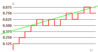
The tracking ADC is one of a number of techniques which employ a DAC in a negative feedback loop. When the DAC output is below the analog input the up/dn input is high and the counter counts up. When the DAC output is over the analog input the up/dn input is low and the counter counts down alternatively.
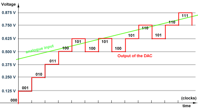
Figure 5: Counting principle of a tracking ADC
The tracking ADC is convenient for slow changes of the analog input only. Up to 2n clock periods required before digital output is valid following a large change in analog input.
Successive Approximation (SAR- ADC)
Although there are many variations in the implementation of a SAR ADC, the basic architecture is quite simple. To implement the binary search algorithm, the n-bit register is first set to midscale (that is, 100... .00, where the MSB is set to '1'). This forces the DAC output (VDAC) to be Vr /2, where Vr is the reference voltage provided to the ADC.
Figure 7: principle of a SAR ADC
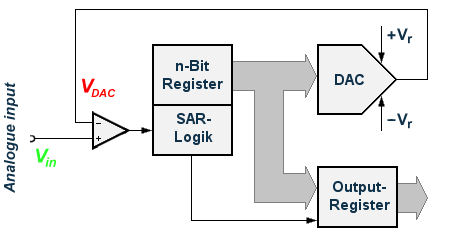
Figure 7: principle of a SAR ADC

Figure 7: principle of a SAR ADC
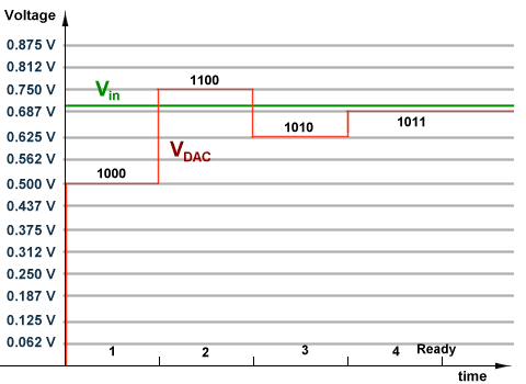
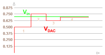
Figure 6: SAR operation (4-bit ADC example)
A comparison is then performed to determine if Vin is less than or greater than VDAC. If Vin is greater than VDAC, the comparator output is a logic high or '1' and the MSB of the n-bit register remains at '1'. Conversely, if Vin is less than VDAC, the comparator output is a logic low and the MSB of the register is cleared to logic '0'. The SAR control logic then moves to the next bit down, forces that bit high, and does another comparison. The sequence continues all the way down to the LSB. Once this is done, the conversion is complete, and the n-bit digital word is available in the output register.
