Zener Diodes
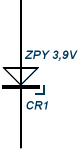
Figure 1: Schematic symbol for Zener diodes
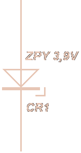
Figure 1: Schematic symbol for Zener diodes
The symbol used to represent Zener diodes is illustrated in figure 1. Note that the polarity markings indicate electron flow is with the arrow symbol instead of against it as in a normal pn-junction diode. This is because breakdown diodes are operated in the reverse-bias mode, which means the current flow is by minority current carriers.
Zener diodes of various sorts are used for many purposes but their most widespread use is as voltage regulators. Once the breakdown voltage of a Zener diode is reached, the voltage across the diode remains almost constant regardless of the supply voltage. Therefore they hold the voltage across the load at a constant level. This characteristic makes Zener diodes ideal voltage regulators, and they are found in almost all solid-state circuits in this capacity.
When a pn-junction diode is reverse biased, the majority carriers (holes in the p-material and electrons in the n-material) move away from the junction. The barrier or depletion region becomes wider, as illustrated in figure 2, and majority carrier current flow becomes very difficult across the high resistance of the wide depletion region. The presence of minority carriers causes a small leakage current that remains nearly constant for all reverse voltages up to a certain value. Once this value has been exceeded, there is a sudden increase in the reverse current. The voltage at which the sudden increase in current occurs is called the breakdown voltage. At breakdown, the reverse current increases very rapidly with a slight increase in the reverse voltage. Any diode can be reverse biased to the point of breakdown but not every diode can safely dissipate the power associated with breakdown. A Zener diode is a pn junction designed to operate in the reverse-bias breakdown region.
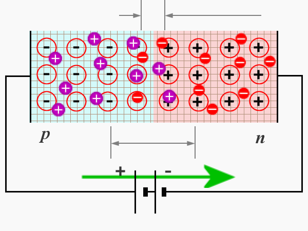
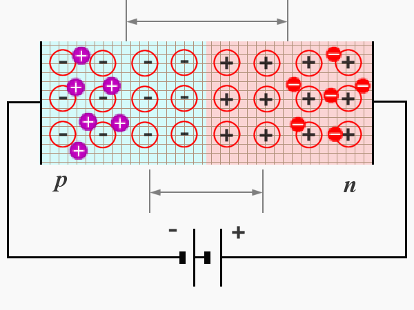
Figure 2: Depletion regions dependent on bias
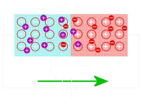
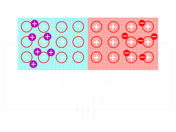
Figure 2: Depletion regions dependent on bias
There are two distinct theories used to explain the behavior of PN junctions during breakdown: one is the Zener effect and the other is the avalanche effect.
The Zener effect was first proposed by Dr. Carl Zener in 1934. According to Dr. Zener's theory, electrical breakdown in solid dielectrics occurs by a process called quantum-mechanical tunneling. The Zener effect accounts for the breakdown below 5 volts; whereas, above 5 volts the breakdown is caused by the avalanche effect. Although the avalanche effect is now accepted as an explanation of diode breakdown, the term Zener diode is used to cover both types.
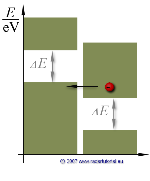
The true Zener effect in semiconductors can be described in terms of energy bands; however, only the two upper energy bands are of interest. The two upper bands, illustrated in figure 3, are called the conduction band and the valence band.
of p-material
of n-material
gap
band
band
band
Figure 3: Energy diagram for Zener diode.
of p-material
of n-material
gap
band
band
band
Figure 3: Energy diagram for Zener diode.
Figure 3 is an energy diagram of a reverse-biased Zener diode. The energy bands of the p and n materials are naturally at different levels but reverse bias causes the valence band of the p material to overlap the energy level of the conduction band in the n material. Under this condition, the valence electrons of the p material can cross the extremely thin junction region at the overlap point without acquiring any additional energy. This action is called tunneling. When the breakdown point of the pn junction is reached, large numbers of minority carriers „tunnel” across the junction to form the current that occurs at breakdown. The tunneling phenomenon only takes place in heavily doped diodes such as Zener diodes.
The second theory of reverse breakdown effect in diodes is known as avalanche breakdown and occurs at reverse voltages beyond 5 volts. This type of breakdown diode has a depletion region that is deliberately made narrower than the depletion region in the normal pn-junction diode but thicker than that in the Zener-effect diode. The thicker depletion region is achieved by decreasing the doping level from the level used in Zener-effect diodes. The breakdown is at a higher voltage because of the higher resistivity of the material. Controlling the doping level of the material during the manufacturing process can produce breakdown voltages ranging between about 2 and 200 volts.
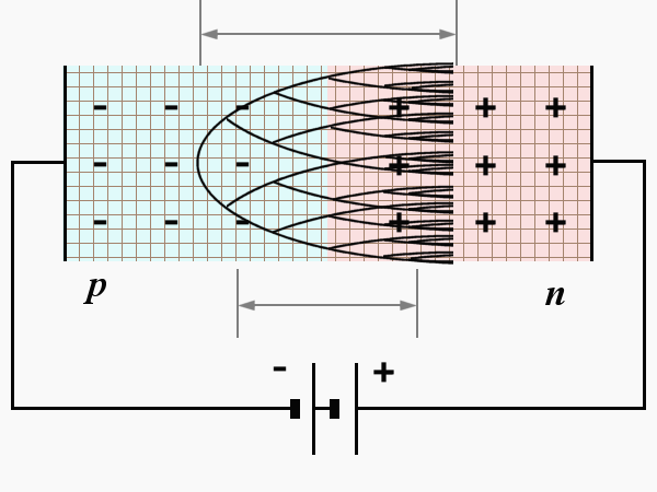
Figure 4: Avalanche multiplication
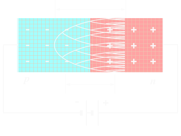
Figure 4: Avalanche multiplication
The mechanism of avalanche breakdown is different from that of the Zener effect. In the depletion region of a pn junction, thermal energy is responsible for the formation of electron-hole pairs. The leakage current is caused by the movement of minority electrons, which is accelerated in the electric field across the barrier region. As the reverse voltage across the depletion region is increased, the reverse voltage eventually reaches a critical value. Once the critical or breakdown voltage has been reached, sufficient energy is gained by the thermally released minority electrons to enable the electrons to rupture covalent bonds as they collide with lattice atoms. The released electrons are also accelerated by the electric field, resulting in the release of further electrons, and so on, in a chain or avalanche effect. This process is illustrated in figure 4.
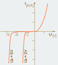
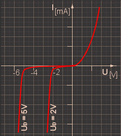
Figure 5: Diagram of a Zener diode
For reverse voltage slightly higher than breakdown UD, the avalanche effect releases an almost unlimited number of carriers so that the diode essentially becomes a short circuit. The current flow in this region is limited only by an external series current-limiting resistor. Operating a diode in the breakdown region does not damage it, as long as the maximum power dissipation rating of the diode is not exceeded. Removing the reverse voltage permits all carriers to return to their normal energy values and velocities.