pnp- Transistor Operation
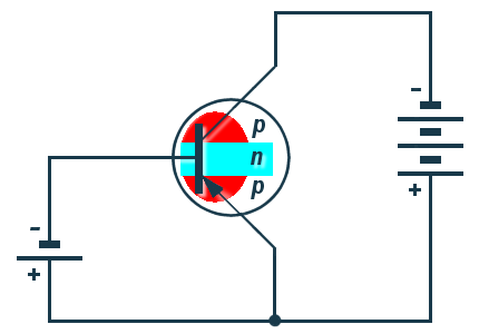
Figure 1: A properly biased pnp transistor
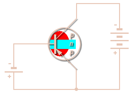
Figure 1: A properly biased pnp transistor
The pnp transistor works essentially the same as the npn transistor. However, since the emitter, base, and collector in the pnp transistor are made of materials that are different from those used in the npn transistor, different current carriers flow in the pnp unit. The majority current carriers in the pnp transistor are holes. This is in contrast to the npn transistor where the majority current carriers are electrons. To support this different type of current (hole flow), the bias batteries are reversed for the pnp transistor. A typical bias setup for the pnp transistor is shown in figure 1.
Notice that the procedure used earlier to properly bias the npn transistor also applies here to the pnp transistor. The first letter (p) in the pnp sequence indicates the polarity of the voltage required for the emitter (positive), and the second letter (n) indicates the polarity of the base voltage (negative). Since the base-collector junction is always reverse biased, then the opposite polarity voltage (negative) must be used for the collector. Thus, the base of the pnp transistor must be negative with respect to the emitter, and the collector must be more negative than the base. Remember, just as in the case of the npn transistor, this difference in supply voltage is necessary to have current flow (hole flow in the case of the pnp transistor) from the emitter to the collector. Although hole flow is the predominant type of current flow in the pnp transistor, hole flow only takes place within the transistor itself, while electrons flow in the external circuit. However, it is the internal hole flow that leads to electron flow in the external wires connected to the transistor.
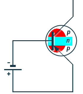
Figure 2: The forward-biased junction in a pnp transistor.
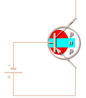
Figure 2: The forward-biased junction in a pnp transistor.
pnp Forward-Biased Junction
Now let us consider what happens when the emitter-base junction is forward biased. With the bias setup shown, the positive terminal of the battery repels the emitter holes toward the base, while the negative terminal drives the base electrons toward the emitter. When an emitter hole and a base electron meet, they combine. For each electron that combines with a hole, another electron leaves the negative terminal of the battery, and enters the base. At the same time, an electron leaves the emitter, creating a new hole, and enters the positive terminal of the battery. This movement of electrons into the base and out of the emitter constitutes base current flow (IB), and the path these electrons take is referred to as the emitter-base circuit.
pnp Reverse-Biased Junction
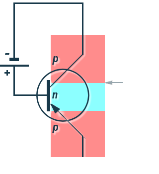
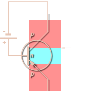
In the reverse-biased junction (figure 3), the negative voltage on the collector and the positive voltage on the base block the majority current carriers from crossing the junction.
However, this same negative collector voltage acts as forward bias for the minority current holes in the base, which cross the junction and enter the collector. The minority current electrons in the collector also sense forward bias-the positive base voltage-and move into the base. The holes in the collector are filled by electrons that flow from the negative terminal of the battery. At the same time the electrons leave the negative terminal of the battery, other electrons in the base break their covalent bonds and enter the positive terminal of the battery. Although there is only minority current flow in the reverse-biased junction, it is still very small because of the limited number of minority current carriers.
bias
junction
Figure 3: The reverse-biased junction in a pnp transistor.
bias
junction
Figure 3: The reverse-biased junction in a pnp transistor.
pnp Junction Interaction
bias
junction
bias
junction
flow
Figure 4: pnp transistor operation.
bias
junction
bias
junction
flow
Figure 4: pnp transistor operation.
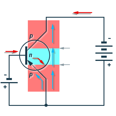
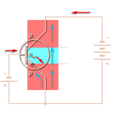
The interaction between the forward- and reverse-biased junctions in a pnp transistor is very similar to that in an npn transistor, except that in the pnp transistor, the majority current carriers are holes. In the pnp transistor shown in figure 4, the positive voltage on the emitter repels the holes toward the base. Once in the base, the holes combine with base electrons. But again, remember that the base region is made very thin to prevent the recombination of holes with electrons. Therefore, well over 90 percent of the holes that enter the base become attracted to the large negative collector voltage and pass right through the base. However, for each electron and hole that combine in the base region, another electron leaves the negative terminal of the base battery (V BB) and enters the base as base current (IB). At the same time an electron leaves the negative terminal of the battery, another electron leaves the emitter as IE (creating a new hole) and enters the positive terminal of VBB. Meanwhile, in the collector circuit, electrons from the collector battery (VCC) enter the collector as Ic and combine with the excess holes from the base. For each hole that is neutralized in the collector by an electron, another electron leaves the emitter and starts its way back to the positive terminal of VCC.
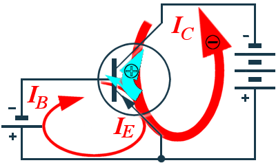
Figure 5: total current flow in the pnp transistor.
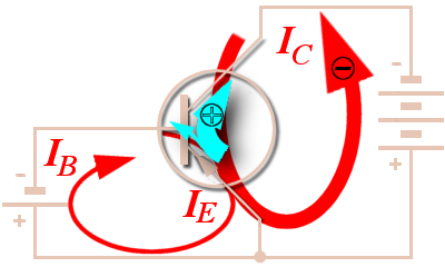
Figure 5: total current flow in the pnp transistor.
Although current flow in the external circuit of the pnp transistor is opposite in direction to that of the npn transistor, the majority carriers always flow from the emitter to the collector. This flow of majority carriers also results in the formation of two individual current loops within each transistor. One loop is the base-current path, and the other loop is the collector-current path. The combination of the current in both of these loops (IB + IC) results in total transistor current (IE). The most important thing to remember about the two different types of transistors is that the emitter-base voltage of the pnp transistor has the same controlling effect on collector current as that of the npn transistor. In simple terms, increasing the forward-bias voltage of a transistor reduces the emitter-base junction barrier. This action allows more carriers to reach the collector, causing an increase in current flow from the emitter to the collector and through the external circuit. Conversely, a decrease in the forward-bias voltage reduces collector current.
