What is a waveguide?
Basics of waveguide theory
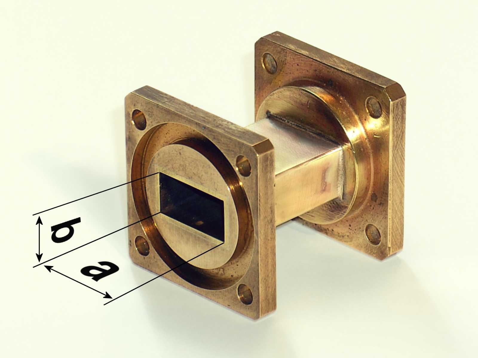
Figure 1: Dimensions of a rectangular waveguide, here's a very short section of waveguide with Choke Joint for frequencies of 18.0 … 26.5 GHz
Figure 1: Dimensions of a rectangular waveguide, here's a very short section of waveguide with Choke Joint for frequencies of 18.0 … 26.5 GHz
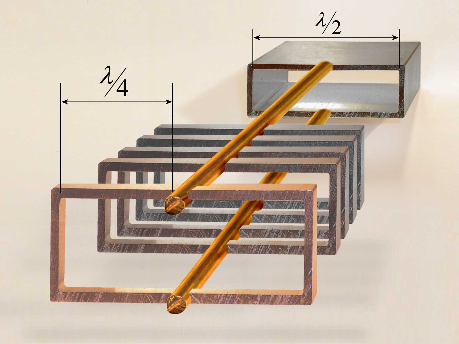
Figure 2: Forming a waveguide by adding quarter-wave sections shorted at one end on each side of a two-wire line.
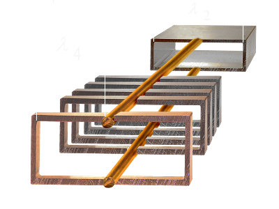
Figure 2: Forming a waveguide by adding quarter-wave sections shorted at one end on each side of a two-wire line.
Basics of waveguide theory
Waveguides are a special form of transmission line used for microwave applications. They are metallic tubes made often of high quality material (copper, brass - partially silvered or gold plated even). In the latest technology these waveguides are produced as electrically copper plated very light carbon fiber composites.[1]
A waveguide may have rectangular, circular or elliptical cross-section. The rectangular waveguide is most commonly used for relatively short connections. Compared to the coaxial lines waveguides have significant advantages. But in practice, these advantages can be used only at frequencies higher than 1 GHz effectively. They have several advantages over two-wire and coaxial transmission lines. The main advantage is that waveguides support propagation with lower loss. The electric and magnetic fields, which are used for the transport of energy, are equal to zero in metal surfaces. Therefore, these fields are confined to the space within the waveguides walls. Also the electromagnetic fields are completely contained within the waveguide and are completely shielded, both from the inside to the outside (radiation losses are kept very low), as well as from outside to inside the waveguide, resulting in a good immunity with very weak wanted signals.
Disadvantages of coaxial cable:
In the frequency range above about 1000 MHz coaxial cables have a number of significant disadvantages in transmission of high power,
such as high attenuation and low flashover resistance.
The attenuation losses caused by their own line capacitances and inductances, as well as the
skin effect
and increase with increasing transmission frequency significantly.
Above 36 GHz coaxial cables can be hardly used due to the high attenuation.
In coaxial cable the flashover and arc resistance is limited by the small distance between the inner and outer conductors.
Such disadvantages are still acceptable for low-power signals but in the high performance range, they lead to unacceptable losses.
Developing the Waveguide
An ordinary two-wire transmission line should be supported at regular intervals by insulators. At the junction with the line, the insulators must have a very high impedance to ground for proper operation. A better highfrequency insulator is a resonant stub, i.e. a matched quarter-wave section of transmission line shorted at one end. With proper matching this kind of insulators will transform the short circuit at a very high impedance connection to the two-wire transmission line.
Figure 2 shows several resonant stubs on each side of a two-wire transmission line. As more stubs are added, each section makes contact with the next, and a rectangular waveguide is formed. The former two-wire transmission line become part of the walls of the waveguide. This waveguide has now a width of λ /2.
Note that the resonant stubs are insulators at only one frequency. This severely limits the bandwidth and the efficiency. Signals can propagate in the waveguide only above a certain frequency. This certain frequency is dependent on the dimensions of the waveguide, particularly of the labeled “a” wall. Propagation conditions exist only if the wavelength to be transferred is less than the so-called cutoff wavelength (λcutoff).
The cutoff wavelength of a rectangular waveguide is obtained from the formula:
| λcutoff = 2 · a | λcut-off = cut-off wavelength [m] a = wider dimension of the waveguide. [m] (see figure 1) |
In fact, waves of this length cannot pass efficiently through waveguides. The waveguide must be about 30% larger than this half-wavelength to operate efficiently. This makes the use of waveguides at frequencies below 1000 megahertz increasingly impractical.
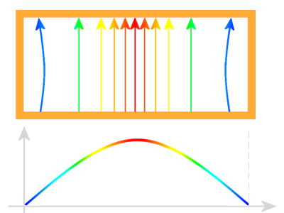
Figure 3: E-field in the waveguide (cross-section, snapshot, TE10- mode)
Waveguides are specified in their dimensions according to Federal Standard 1037C The specifications and descriptions correspond to those of the IEC 153 and the German DIN 47302. For a rectangular waveguide, the narrower wall “b” is half the size of the wider wall “a”. The waveguide section in Figure 1 is made of an extruded rectangle tube of brass, designated to as WR 42 type. The waveguide designation “WR” stands for “Waveguide Rectangular”, and the number is the wider inner dimension width of the waveguide in hundredths of an inch.
- Whose side “a” is thus exactly 0.42 inches, ie 0.42 x 25.4 mm = 10.67 mm wide.
- The width of the side “b” is exactly half the size, ie 5.34 mm.
- Its lower cutoff frequency is 14.051 GHz. Low-loss transmission of frequencies start but only from 30% above this cutoff frequency.
- An upper cutoff frequency is determined by the propagation condition for an wrong mode whose lower cutoff frequency is 28.102 GHz in this waveguide. The upper cutoff frequency for the basic mode is about 5% lower.
- The corresponding frequency band for this type of waveguide is between 18.0 GHz and 26.5 GHz for low-loss transmission.[2]
field
Figure 3: General propagation modes in the waveguide
field
Figure 4: General propagation modes in the waveguide
Propagation of electromagnetic waves in the waveguide
If energy is fed into a waveguide, then an electric field (E- field) is formed in the center of the wider wall “a”. This electric field is strongest in the center of the waveguide and decreases in the direction of the narrower wall “b”. It has a sinusoidal shape in cross-section. By the electric field also arises a magnetic field. However, the magnetic field cannot stand vertically on a metallic conductor. As propagation direction remains only the direction which is passed through the waveguide.
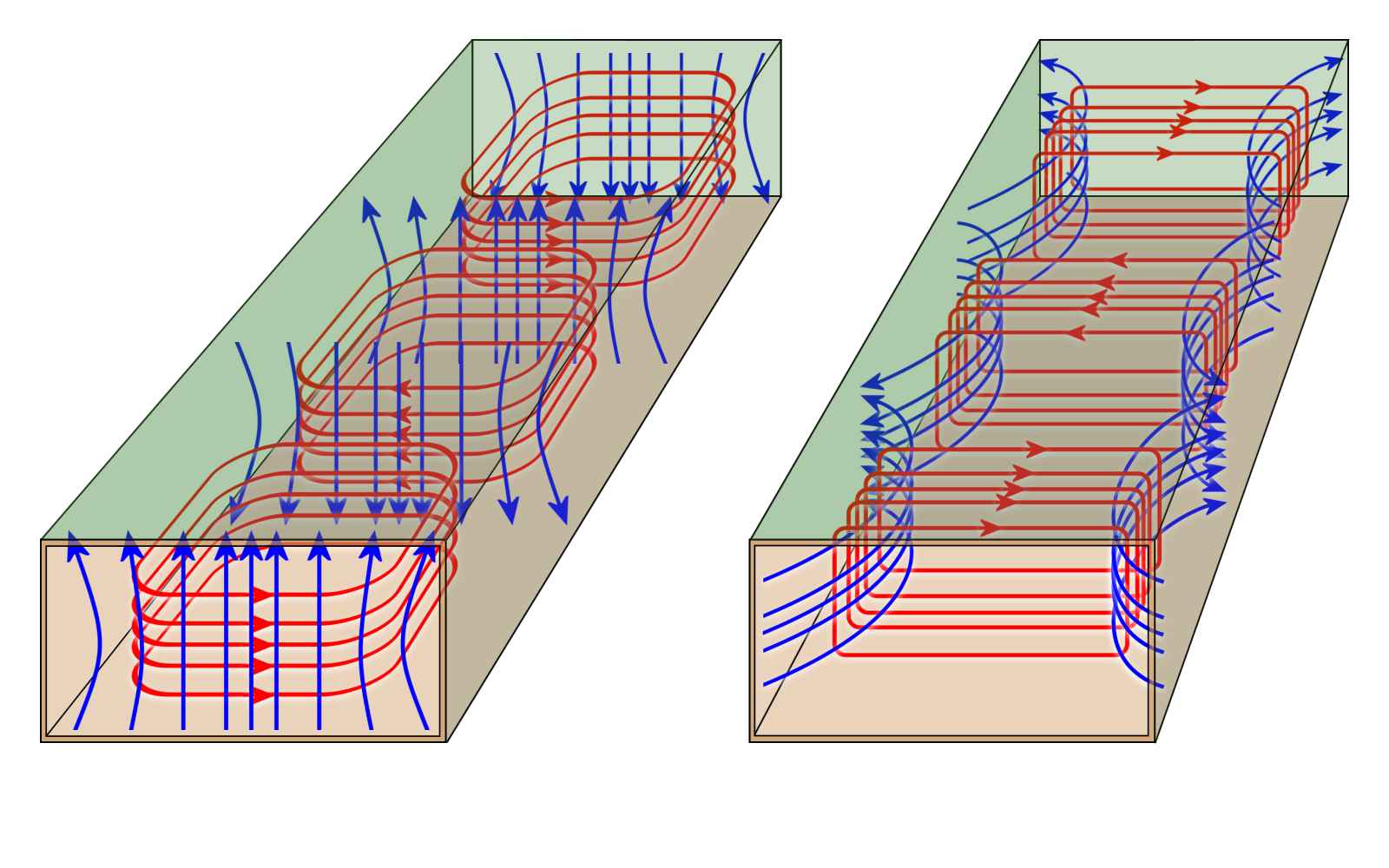
The electric field changes over time with the frequency, and has in the longitudinal direction of the waveguide maxima and minima in the distance of half the wavelength. High frequency energy that is fed into a waveguide, generates an electromagnetic transverse wave (TEM mode) whose electric and magnetic fields are perpendicular to each other. The electric field is established between the two wider waveguide walls, the magnetic field lies between the two narrower walls. These fields do not remain in the respective states. Considered over the timeline, they change the intensity and polarity in the rhythm of the input signal. This electromagnetic wave propagates in the waveguide at near-light speed.

Figure 4: E-field in the waveguide (cross-section, snapshot, TE10- mode)
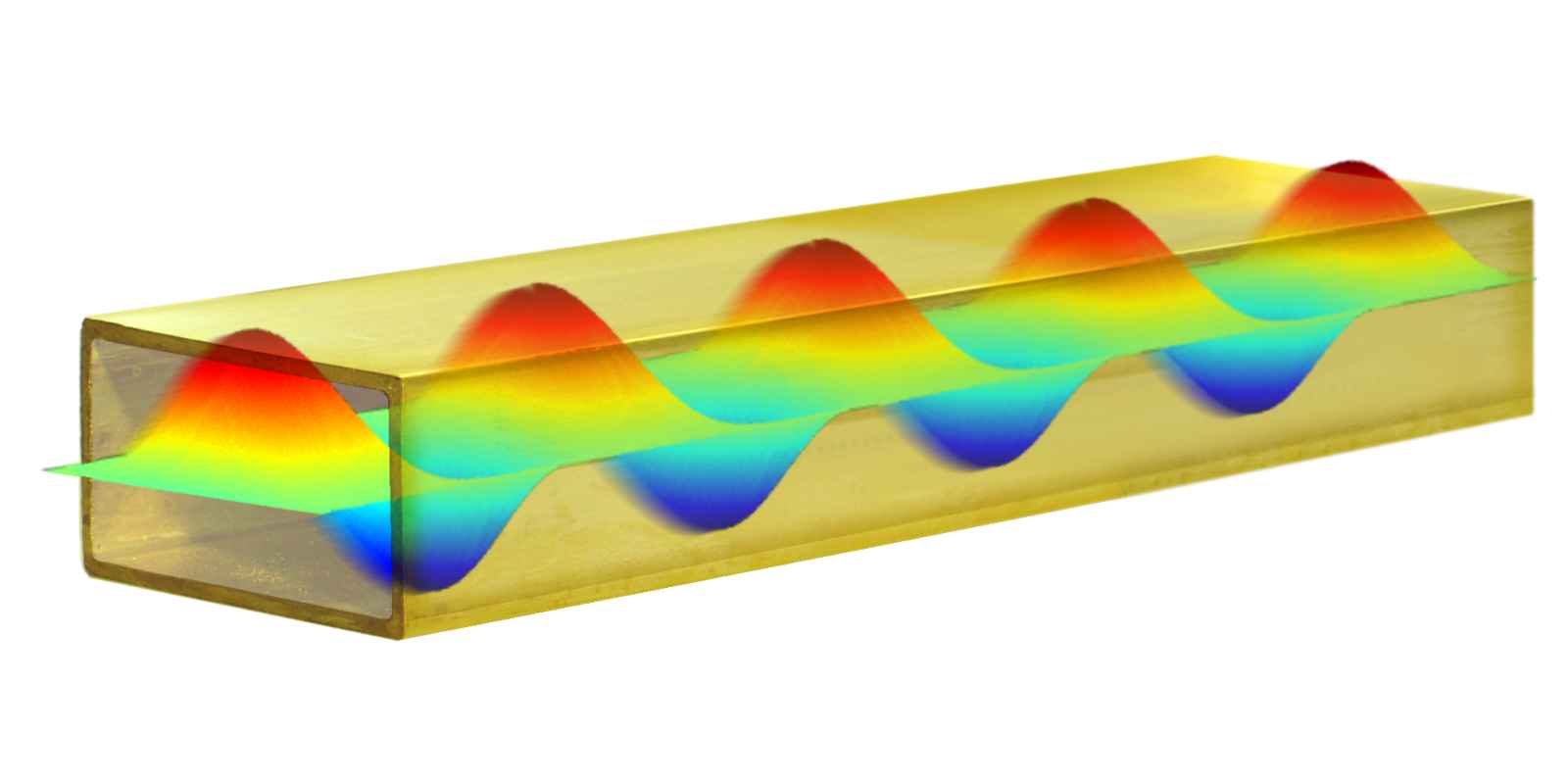
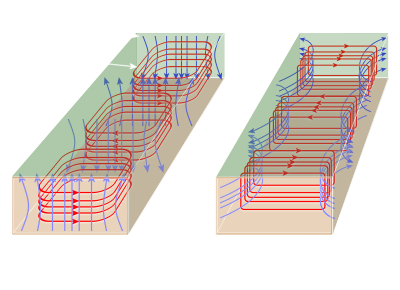
Figure 5: Three-dimensional view of the electric field for the TE₁₀– mode in a rectangular waveguide
Figure 5: Three-dimensional view of the electric field for the TE₁₀– mode in a rectangular waveguide
Älteres Bild nicht mehr in Großformat:
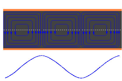
Figure 6: H field in the waveguide (top view, snapshot)
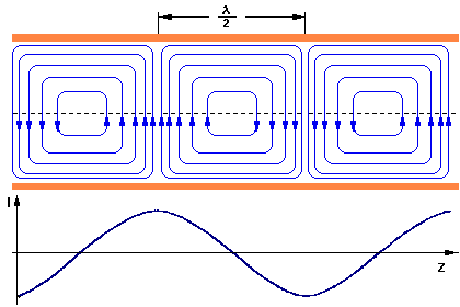
Figure 6: H field in the waveguide (top view, snapshot)

Figure 6: H field in the waveguide (top view, snapshot)
The electric and the magnetic field change its strength and polarity permanently, but they are always perpendicular to each other locally. If the electric field is in propagation direction, it is called an E-wave or TM wave (Transverse Magnetic). If the magnetic field is in propagation direction, it is called an H-wave or TE wave (Transverse Electric).
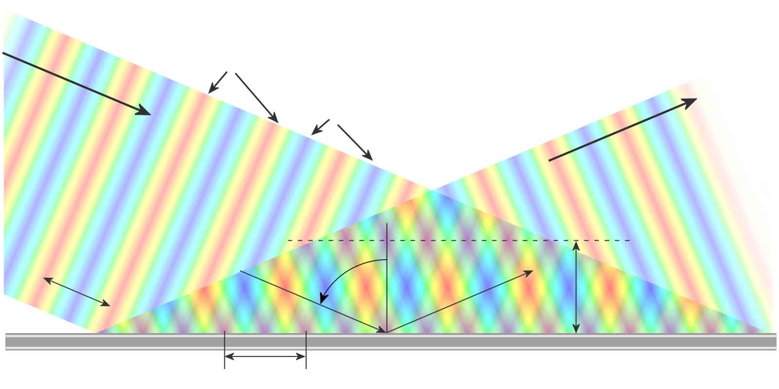
wall “a”
Figure 6: Reflection of a wave obliquely incident on a metal wall
Propagation by multiple reflection
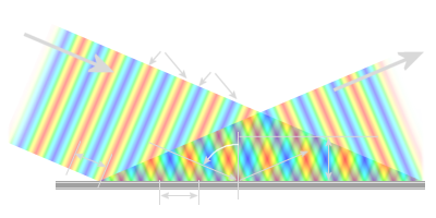
The wave propagation in the waveguide can be partly explained with the help of geometrical optics. The properties of the waves in a waveguide can be derived from those of a plane wave in free space. Figure 6 shows the reflection of a plane wave having a wavelength of λ0 in a metal wall at an angled incidence (here is φ = 67°). The electric field E is perpendicular to the plane of representation here and can therefore only be marked in different colors. The wave crest (with +Emax) is colored red and the wave trough (with −Emax) in blue. The green color symbolizes the zero line.
The angle of incidence is equal to the angle of reflection. During the reflection at the wall, the wave undergoes a phase shift of 180 degrees. The superposition of the two waves can be seen in the image because the formation of local minima and maxima as much red or blue colored areas at a certain distance from the metal wall. At a distance of
| a = 0.5 | λ0 | (2) |
| cos φ |
for the electric field E there is a line of complete annihilation parallel with the metallic wall. The positive wavefront of the incident wave (colored in red) coincides with the negative wave front of the reflected wave (colored in blue). (Here in the image this results in magenta by the additive color mixing. Energetically correct these areas should be green.) The picture moves permanently to the right with the arrival of the incident wave.
You could set up a second metal wall along this line in the distance “a”, without any change in the situation up to the wall. The process of reflection is repeated at this second wall, replacing the permanent exposure of the incident wave. Positive and negative maxima of the wave arise between these two walls (as before only at one wall). These migrate as “packages” to the right with the so-called phase velocity or group velocity. These “packages” would correspond to a 3-dimensional representation shown in Figure 5. These two walls (the drawn wall at the bottom of the graph and the only conceptually be presented wall at the level of the horizontal line) corresponding to the walls “b” of the waveguide.
It is also imaginable from this graph that optimum wave propagation in the waveguide is only possible at an optimum angle of incidence of the incident wave. The optimum width of the waveguide side "a" is also dependent on this angle of incidence φ, and the wavelength λ0 of the incident wave.
Wavelength in the waveguide
Practically, in the waveguide arise voltage minima and maxima by multiple interference of reflected on the walls energy parts. The migrating to the right “packages” have a different distance in their maxima with each other, than the wavelength λ0 in free space. This distance corresponds
| λh = | λ0 | (3) |
| sin φ |
Therefore, the wavelength of an oscillation in the waveguide λh is different from the wavelength of the same oscillation in free space λ0. Unfortunately, this angle is difficult to measure. From the ratio of the wavelength to the optimum angle of incidence, these dependencies can be linked. The wavelength in the waveguide now depends on the ratio of the dimension of the waveguides wall a to the wavelength in free space:
.png) (4)
(4)
The result is a phase velocity which propagates at a uniform oscillation with a by a factor of sin φ higher speed than the speed of light. Therefore, the wavelength in the waveguide λh is often significantly greater than in free space. An energy transport (and thus also a local change of the oscillation by, for example, modulation), however, still spreads with a speed, which is less than the speed of light.
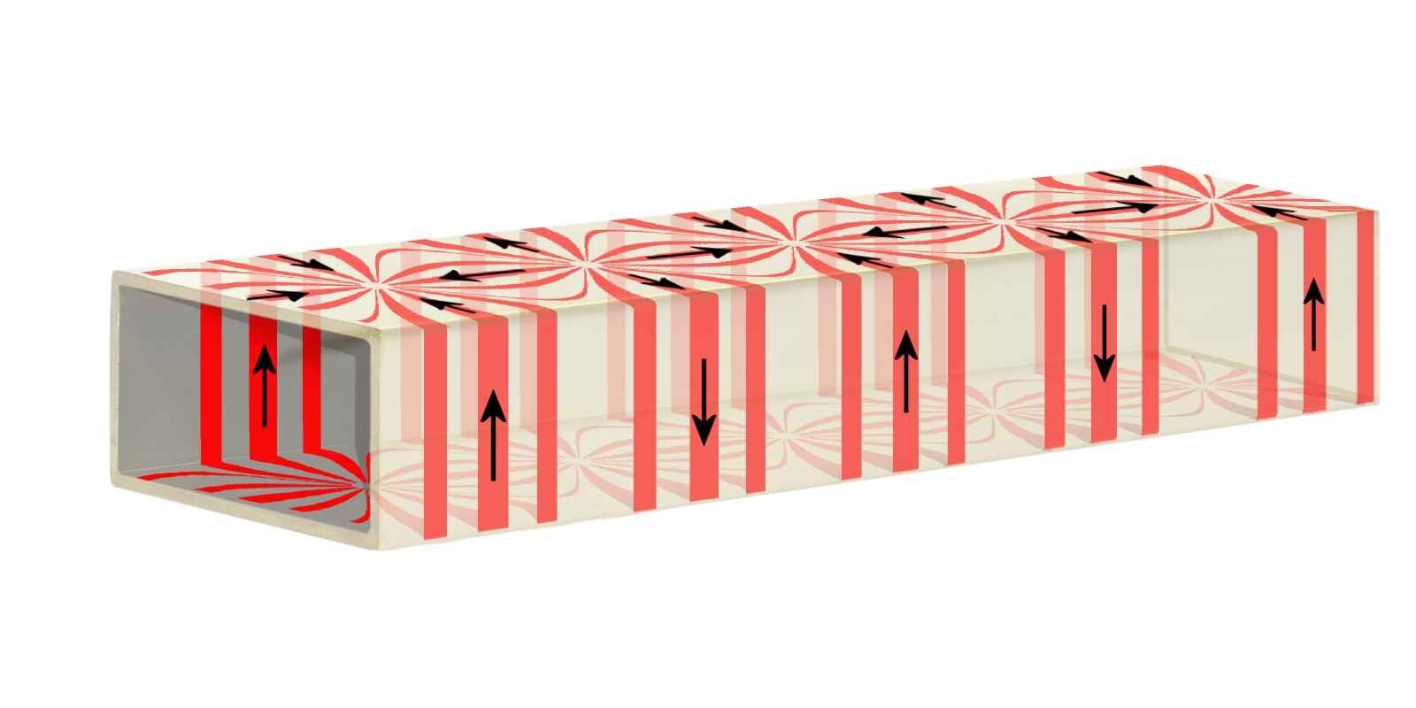
Figure 7: Illustration of a wall currents TE₁₀-wave (snapshot). In a traveling wave, the image moves with approximate speed of light in the direction of propagation.
Figure 7: Illustration of a wall currents TE₁₀-wave (snapshot). In a traveling wave, the image moves with approximate speed of light in the direction of propagation.
Reasons for the attenuation
The attenuation in waveguides is strongly frequency dependent. A waveguide operating at the cutoff frequency, still has a relatively high attenuation. It reaches a minimum only with the increase in frequency. This area remains almost constant over a certain range but increases thereafter. Decisive factor for the good conductivity of the rectangular waveguide is its dimension (wall “a”) with respect to the frequency to be transmitted. If the wavelength is too large, the voltage maxima do not have enough space: they will be smaller. Higher frequencies need waveguides with smaller dimensions and vice versa.
The attenuation of the waves are carried out by wall current losses. Figure 7 shows the distribution of wall currents of a TE₁₀–wave. The wall currents flow on the bottom wall and the cover wall in the middle in the propagation direction. Additional cross currents flow toward the edges. The attenuation constant of the waveguide for a given mode could be estimated from the calculation of the surface integral over the wall current density.
The wall currents flow only on the inside of the waveguide. Usually the waveguides walls are made of polished brass. The wall interior surface must have excellent conductivity. The surfaces can also silvered or (from about 40 GHz) even be gold plated. Pollution on the surface have an impact as additional attenuation.
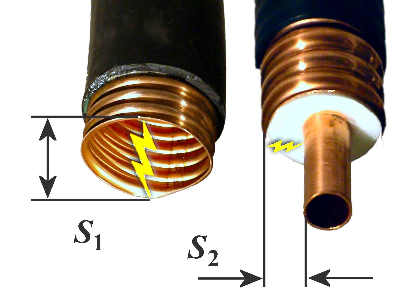
Figure 8: At approximately the same diameter the waveguide has significantly improved dielectric strength
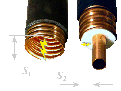
Figure 8: At approximately the same diameter the waveguide has significantly improved dielectric strength
Dielectric strength
The the flashover and arc resistance of a waveguide depends on the spacing of the waveguides walls, that is, small cross-section waveguides (for high frequencies) have a lower breakdown strength as a waveguide with a large cross-section. For rectangular waveguides is relevant the smallest distance, ie the length of the wall “b”. This is also dependent on the air humidity in the interior of the waveguide. In order to improve it at higher transmission powers, an overpressure is generated inside the waveguide with the help of specially dried air. If the waveguide is slightly leaky at one point, the dry air flows out and moisture cannot penetrate.
Applications
Waveguides are used in
- high-power transmitters;
- radar equipment;
- microwave ovens;
- and also in Low Noise Block converters (LNBs) which are used in TV- satellite dishes.
References:
- Press Release of the Fraunhofer-Instituts für Schicht- und Oberflächentechnik
- Raw Waveguide Information (Technical data for commercial waveguides)

